Products
Academic And Industrial R&D Professional Inspection System

Academic And Industrial R&D Professional Inspection System

JadeSA-WBG

Non-contact 3D Stress Inspection and Analysis System for WBG Materials

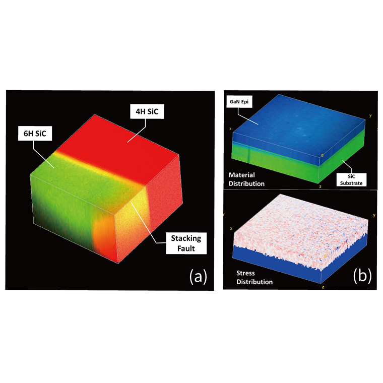
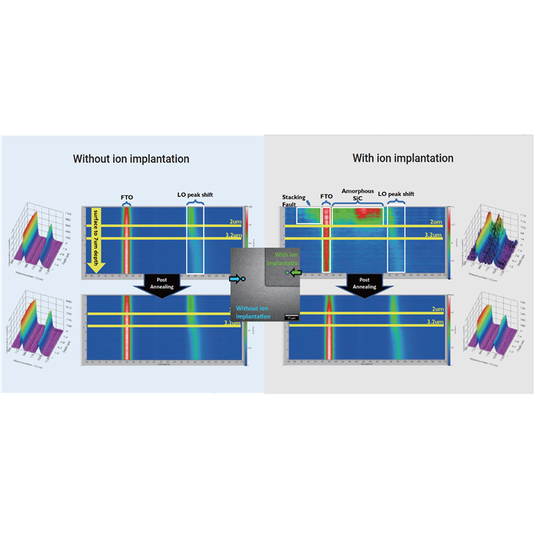
▪ Effectively reflect the intrinsic property of WBG materials ‒ stress distribution on surface and in depth ▪ Good for monitor the stress distribution and polytype uniformity of SiC substrate, homogeneous and heterogeneous epi wafer, and device process review

Features

  • Advanced 3D Raman inspection technology
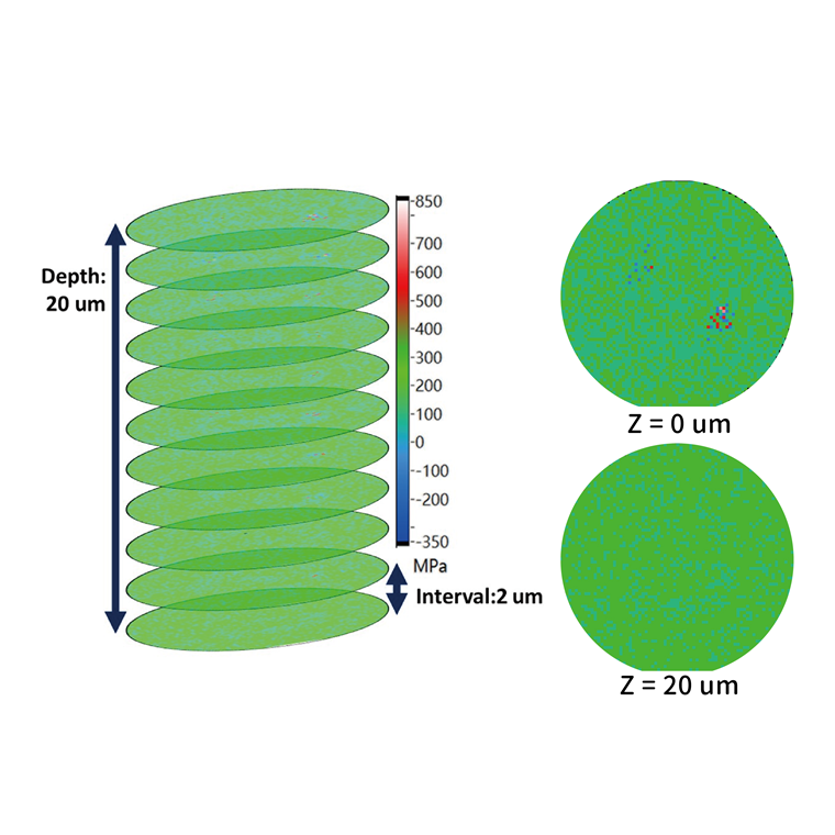
  • Effectively reflect the intrinsic property of WBG materials ‒ stress distribution on surface and in depth
  • Capable of providing the percentage of unexpected polytype in the wafer
  • Capable of performing whole wafer scan at specific depth with stress mapping
  • Capable of performing MicroArea 3D stress mapping
  • Capable of performing 3D polytype analysis
  • Good for monitor the stress distribution and polytype uniformity of SiC substrate, homogeneous and heterogeneous epi wafer, and device process review
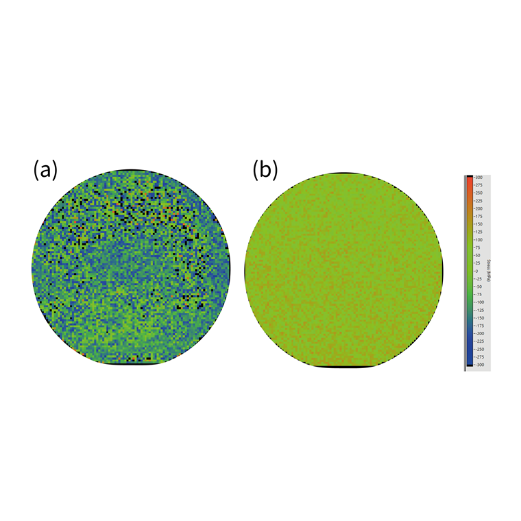
  • Applied to 2”, 4”, 6”, 8” substrates

Specifications

#FIRST NAMELAST NAMEUSER NAMEDATE
Available samplesSiC substrate, SiC on SiC, GaN on Si, GaN on SiC, GaN substrate
Available wafer size2", 4", 6", 8"
Inspection itemWhole wafer stress mapping, Micro area stress mapping, Polytype Detection (4H, 6H, 3C SiC)
Whole wafer stress scan speed40 mins / layer ( @4" wafer, 2 mm step size )
Whole wafer stress mapping axial resolution1 μm
Micro area stress mapping FOV250 μm
Micro area stress mapping resolutionUp to 512 x 512

Contacts

+886-2-2697-5562
+886-2-2697-3927
info@southport.com.tw
18F-1, No. 95, Sec. 1, Xintai 5th Rd., Xizhi Dist., New Taipei City,Taiwan
南方科技股份有限公司 Southport Corporation
Copyright © 2014-2024+ All Rights Reserved.
Features
Specification
Expansion Modules