Pillars-Addressed Area
Academic And Industrial R&D Inspection System

Academic And Industrial R&D Inspection System

JadeMat - Material Inspection System

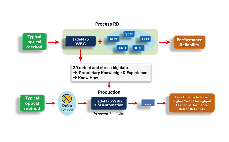
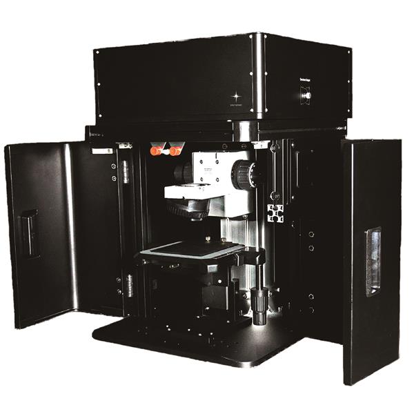
JadeMat is a high-speed advanced optical inspection system that combines spectrum and image in One. It solves the problem of not being able to obtain both the material image and its spectrum in the ROI (Region of Interest) simultaneously. JadeMat can achieve a more comprehensive and precise description of material characteristics for advanced analysis. The introduction of non-destructive inspection technology allows a variety of sensitive or precious samples to maintain their structure and properties during the inspection process, which leads to more accurate and complete 3D material signals.

Nano and 2D Material

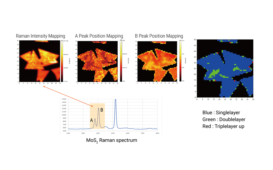
JadeMat is the best optical inspection system for nanomaterials. It performs high-speed and high-resolution optical images, ultra-high-speed spectral image mapping, and accurate micro-area measurement. Features such as fully automatic light path switching, auto-focusing, rapid identification of the number of layers in the research of two-dimensional materials, and laser micro-area annealing/modification shaping, etc., are just what you need. Convenient spectral imaging software analysis including wavelength, intensity, half-height width, band image and overlay, statistical analysis of spectral information, etc., further facilitate your research. JadeMat can be upgraded with advanced OAM and other functional modules to further open up the space for cutting-edge material research!
Wide band gap Semiconductor

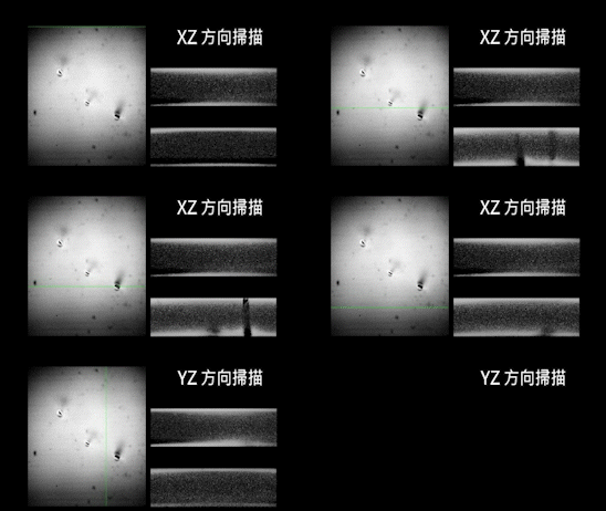
The first innovative development capable of carrying out under-the-surface inspection for compound semiconductors (such as GaN and SiC) with stress, depth structure, and defect information! The lattice structure (such as 3C, 4H, or 6H structure for SiC), the dislocation, and the stress distribution can be detected by fast 3D Raman spectroscopy. With non-linear second harmonic generation (SHG), fast 3D imaging concerning a variety of typical defects, their positions, and structure under the surface of the sample can also be carried out to further examine the quality of the substrate and epitaxial layer of the compound materials.

Perovskite

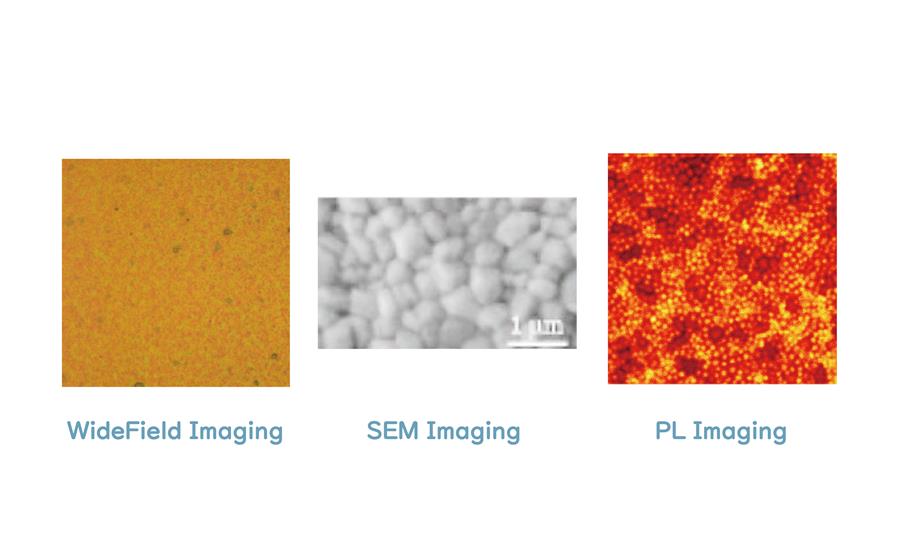
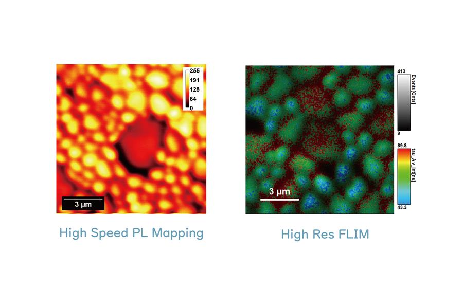
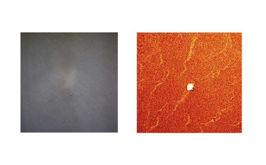
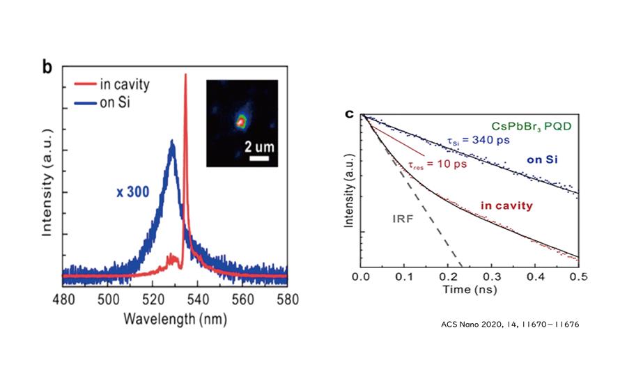
The best perovskite material inspection system you can find. It provides high-speed and high-resolution crystal grain spectral image and non-destructive spectrum measurement mode with large-scale high-speed photoelectric efficiency, all in one system and one setup. Fully automatic light path switching, auto-focusing, convenient spectral image, and non-destructive, surface and depth observation. Fluorescence imaging, white light imaging, fluorescence spectroscopy, Raman spectroscopy mapping, transient spectroscopy (TRPL), and FLIM are what you can also get. Good for the magnetic field, low temperature, and high-temperature environment control.

MicroLED

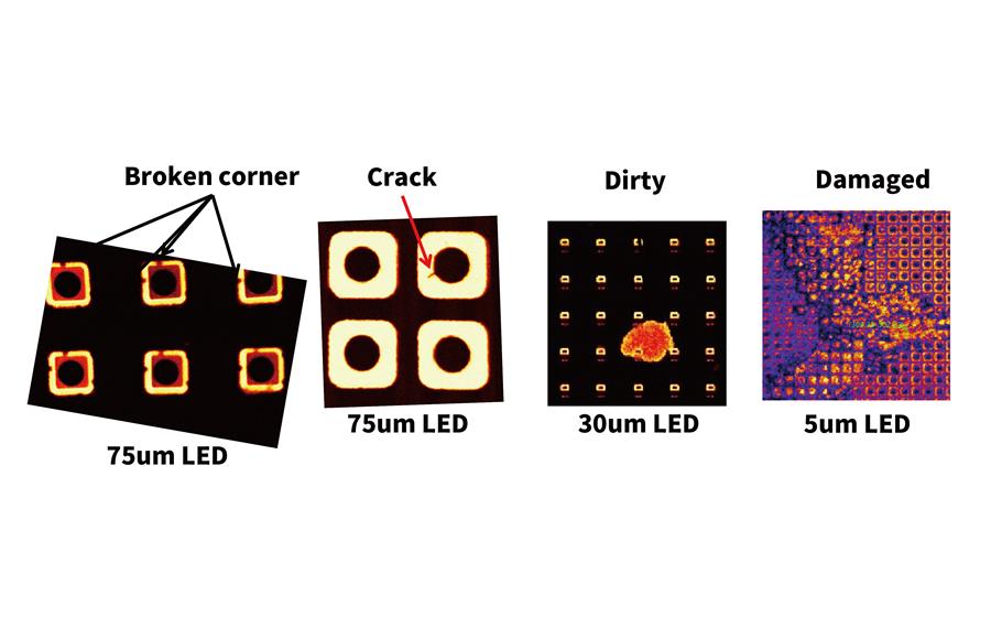
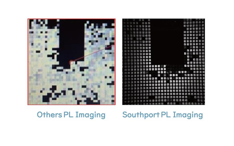
The best MicroLED optical inspection system. Through sub-micron space analysis and sub-nano spectral analysis, JadeMat can quickly detect epitaxial uniformity, chip quality before the mass transfer, and panel quality after mass transfer. Epitaxy inspection items include: Bow / Warp, wavelength, intensity, half-height width, dominant wavelength, reflectivity, film thickness; crystal grain inspection items include: peak wavelength, peak intensity, half-height width, dominant wavelength, CIE XY; Panel inspection items are: EL yield, interlayer defects. With the P-EL detection method, there is no need to go through the spot measurement to get the prediction of the EL lighting status. The capabilities are the core of the Micro LED automated mass inspection system!

Single-Photon Source Detection

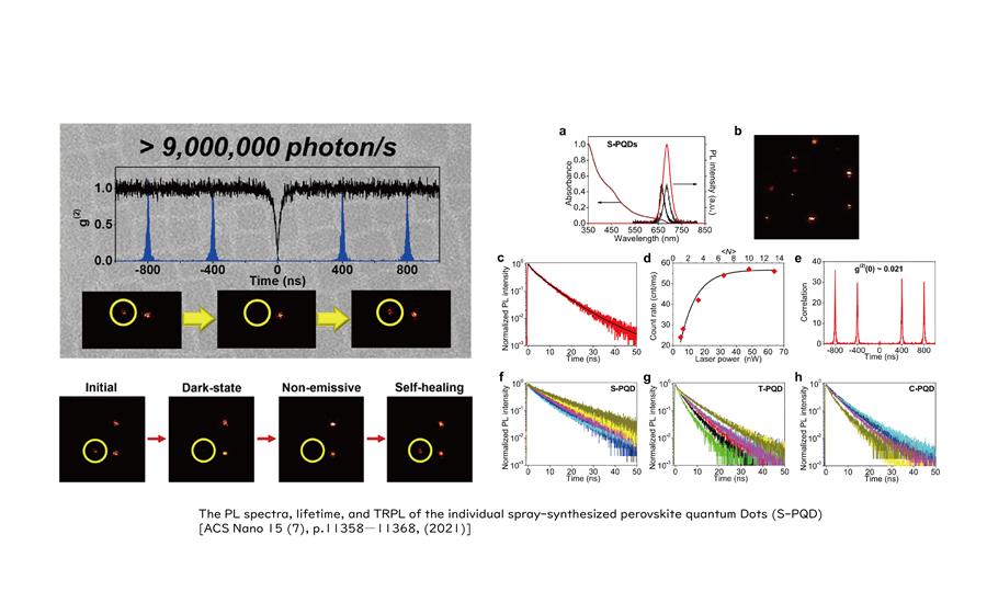
Using clear images combined with accurate optical positioning information is the best detection scheme for material properties of quantum emitter! It can quickly focus on the emitting core of the quantum light source and directly measure the quantum source both qualitatively and quantitatively through a highly-sensitive and low-noise single-photon detection module. Therefore, it is easy to upgrade the research of quantum technology!

Quantum Dot Inspection

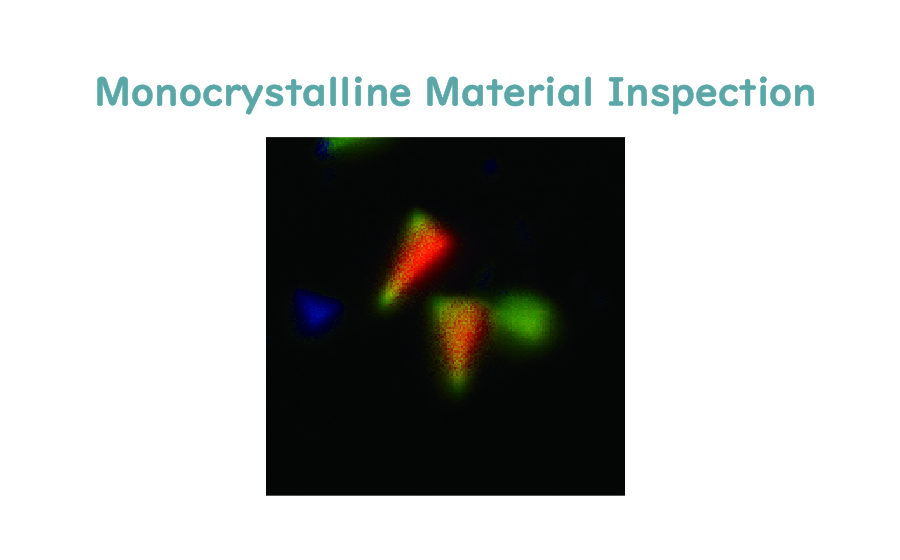
It is the best quantum dot detection system. With high-resolution fluorescent imaging and non-destructive measurement, the system can quickly find quantum dots. At the same time, through the speed of light positioning method, it can achieve fast alignment, accurately switching between different quantum dots, and match the spectrum and time spectrum modules. Therefore, all the optical characteristics of each quantum dot can be measured. This allows users to conduct accurate, high-speed, and multiple analysis research!

Contacts

+886-2-2697-5562
+886-2-2697-3927
info@southport.com.tw
18F-1, No. 95, Sec. 1, Xintai 5th Rd., Xizhi Dist., New Taipei City,Taiwan
南方科技股份有限公司 Southport Corporation
Copyright © 2014-2024+ All Rights Reserved.